Plasmonics
It has been known since Roman times, that by mixing silver and gold colloids with glass, the latter acquires vibrant colors. This property was widely utilized throughout the centuries to decorate windows in churches and cathedrals (stained glass). In the 19th century, Michael Faraday was probably the first to study the colors of gold particles in a scientific way [1]. However, the secret of stained glass was not unveiled until a German physicist Gustav Mie presented a theory that explained the optical properties of spheres in 1908 [2]. The so-called Mie theory showed that the sphere size, its dielectric function and the refractive index of the surrounding medium determines the color of metal nanoparticles, for example gold or silver. The electronic excitations responsible for these vibrant nanoparticle colors are now known as localized surface plasmons (LSP’s) or particle plasmons.
In the past two decades the plasmonics area experiences a remarkable and nearly exponential growth. It would be a difficult task to mention all applications related to the nanoplasmonics field. However, probably the largest application areas would be biosensing, medical diagnostics and biomedical research, nanoantennas, plasmon waveguides, metamaterials, surface-enhanced Raman scattering spectroscopy and optical devices.
Surface Plasmons
Before going into localized surface plasmons (LSP’s), it is worthwhile discussing surface plasmons (SP’s). A surface plasmon polariton (SPP) is a coupled charge-density electromagnetic wave that is bound to the interface between a material with a negative dielectric constant (for instance, silver or gold) and a material with a positive dielectric constant (for instance, air or glass).
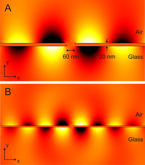
The SPP’s have attracted significant interest because it opens new ways to manipulate light on nanometer scales. Considerable efforts have been made towards integrated optical devices and circuits and future all-optical photonic chips. Even thought the SPP propagation along metal surfaces can only reach a few tens of micrometers [3], plasmon based components such as mirrors [4], waveguides [5] and interferometers [6] have been successfully fabricated. The SPP’s can also be used to observe molecular binding events with a detection limit of approximately 0.003 nm in adsorbate thickness [7]. A great number of techniques have been used to launch SP’s. In Figure 1, a theoretical example using a 60 nm slit in 20 nm thick Au film is shown.